


Производитель может поднять цены — запросите коммерческое предложение сейчас, и мы зафиксируем за вами текущую цену.
-
 Привезем под заказ
 -
 Срок поставки с завода 6-8 недель
Back-gated LOFET Circuit Substrate FIPMS267-1PAK
- Код:
- FIPMS267-1PAK
- Производитель:
- Sigma-Aldrich

- Производитель:
- Sigma-Aldrich
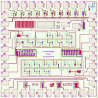
Structure classes: transistors, inverters, and ring oscillators, additional technology test structures, basic circuits
Die size: 15 x 15 mm2
No. of dies: 56
No. of pads: 39 + 2
Pad size: 1200 x 800 µm2
Gate oxide: 200 nm ± 10 nm
Structured layers: 3 (gate, contacts, source/drain)
Gate layer: Ti/TiN, Rs about 10/sq
Contacts: standard 20 x 20 µm2, R around 20
Top layer: 70 nm Au with 10 nm high work function adhesion layer (ITO), by lift-off technique, Rs about 0.65 /sq/ 0.45 /sq
Documentation: included in shipment
Shadow mask: possible, but not required
Probecard: possible, but not required
Protection: resist protection layer (AR PC 5000/3.1, soluable in AZ-thinner or acetone)
Transistors (11)
Connections:
- shared gate (2 pads on different chip sides)
- shared source (2 pads on different chip sides)
- drain for each transistor
- transfer and output characteristics for each transistor to evaluate new organic semiconductors or to monitor organic material fabrication
- designed for parameter extraction to obtain simulation models
Inverters (4)
All 4 inverters are used within the ring oscillator stages or output drivers
Connections
- shared gate IN for the active transistors (2 pads on different chip sides)
- shared gate GEX for the load transistors (2 pads on different chip sides)
- shared VSS
- VDD and output OUT pads for each inverter
- Layout designed for single transistor separation
- Channel length of all transistors: L=5 µm
- Inverter (input/output) characteristics for rapid monitoring of organic materials
- Supply voltages on VDD and VSS (e.g. for p-type organic material: most positive voltage connected to VDD and ground connected to VSS)
- Voltage on IN (gate of active transistor) with value between VDD and VSS
- Different voltage on GEX (gate of load transistor) changes driver/load ratios
- Important: measure output voltages with high impedance volt meter
Ring oscillators (4)
- Connections - left edge (2 ring oscillators)
- shared gates (GATE_1_2) for all load transistors
- shared VSS
- VDD and output OUT pads for each oscillator
- shared gates (GATE_3_4) for all load transistors
- shared VSS
- VDD and output OUT pads for each oscillator
- 7 or 15 ring stages
- Simple inverter layout or inverter layout, designed for single transistor separation
- Different driver/load ratios
- Channel length of all transistors: L=5 µm
- Measure result: oscillation frequency on OUT and calculated inverter delay
- No input signal required
- Supply voltages on VDD and VSS (e.g. for p-type organic material: most positive voltage connected to VDD and ground connected to VSS)
- Different voltage on GEX (gate of load transistors) changes driver/load ratios
- Changing these voltage (more positive or more negative than VSS) triggers oscillation
- Measure output: high impedance oscilloscope probe required
To guarantee a complete cleaning of the wafer / chip surface from resist residuals, please rinse by acetone and then dry the material immediately by nitrogen (compressed air).
Recommendation for material characterization:
If gate currents appear during the characterization of the field effect transistors, considerable variations could occur at the extraction of the carrier mobility. Therefore it is necessary to check the leakage currents over the reverse side (over the chip edges) of the OFET-substrates.
Resist layer was applied to prevent damage from scratches.
Expiration date is the recommended period for resist removal only. After resist removal, the substrate remains functional and does not expire.
| form | chips (diced) |
| packaging | pack of 1 (wafer of 56 diced chips) |
| storage temp. | 15-25°C |
Получите коммерческое предложение в течение 1 часа
Менеджер подготовит коммерческое предложение и позвонит, если понадобится уточнить детали вашего заказа

С 2010 года мы поставляем оборудование с заводов Европы. Берем на себя все — от подбора оборудования до внедрения на предприятии

Все сотрудники имеют высшее образование, закончили ведущие химические вузы страны, такие как РХТУ им Менделеева.

У большинства компаний срок ожидания составляет 10-12 недель.

Оборудование хранится на сухом отапливаемом складе, где поддерживается ровная температура.

Работаем с PonyExpress и Деловыми линиями. Вы также можете выбрать свою транспортную компанию или забрать товар со склада в Москве.

В случае любых неполадок за свой счет выполним ремонт в сервисном центре или на заводе-изготовителе. Или бесплатно заменим прибор на новый.

Производим пуско-наладку оборудования, валидацию, обучение сотрудников. Если нужно, привлекаем инженеров с заводов- изготовителей.
Отзывы


В числе наших клиентов организации
из разных отраслей
Производитель может поднять цены — запросите коммерческое предложение сейчас, и мы зафиксируем за вами текущую цену.
-
Привезем под заказ
-
Срок поставки с завода 6-8 недель
Back-gated LOFET Circuit Substrate FIPMS267-1PAK
- Код:
- FIPMS267-1PAK
- Производитель:
- Sigma-Aldrich


